
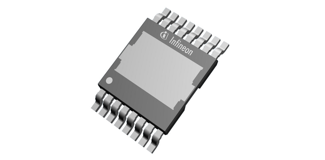
Infineon package reference image
IPTC017N10NM5LF2 is Infineon’s best-in-class OptiMOS™ 5 Linear FET 2 100 V in the TO-Leaded top-side package. Offering the industry’s lowest R<sub>DS(on)</sub> and wide SOA at 25˚C. With the combination of OptiMOS™ 5 Linear FET 2 technology and TOLT package, the IPTC017N10NM5LF2 is designed to provide highest power density, for inrush current protection applications such as hot-swap, e-fuse, and within battery protection in Battery management systems (BMS).
Key Specifications
| Complete manufacturer part number | IPTC017N10NM5LF2ATMA1 |
|---|---|
| Manufacturer | Infineon Technologies |
| Description | IPTC017N10NM5LF2 is Infineon’s best-in-class OptiMOS™ 5 Linear FET 2 100 V in the TO-Leaded top-side package. Offering the industry’s lowest R<sub>DS(on)</sub> and wide SOA at 25˚C. With the combination of OptiMOS™ 5 Linear FET 2 technology and TOLT package, the IPTC017N10NM5LF2 is designed to provide highest power density, for inrush current protection applications such as hot-swap, e-fuse, and within battery protection in Battery management systems (BMS). |
| Package / case | PG-HDSOP-16-2 |
| Product category | N-channel MOSFETs |
| Pins | 16 |
| Operating Temperature (manufacturer catalog) | -55 °C to 175 °C |
| Polarity (manufacturer catalog) | N |
| QG (manufacturer catalog) | 165 nC |
| Switch Type (manufacturer catalog) | MOSFET |
| Technology (manufacturer catalog) | OptiMOS™ 5 LF 2 |
| VGS(th) (manufacturer catalog) | 3.1 V |
| VGS(th) range (manufacturer catalog) | 2.3 to 3.9 V |
| QG [typ @10V] (manufacturer family record) | 165 nC |
| VGS(th) (manufacturer family record) | 3.1 V |
| VGS(th) minimum (manufacturer family record) | 2.3 V |
| RDS (on) maximum [@10V] (manufacturer family record) | 1.7 mΩ |
| VDS maximum (manufacturer family record) | 100 V |
| VGS(th) maximum (manufacturer family record) | 3.9 V |
| In stock | Contact for availability |
| Unit price | Request a quote |
| Lead time | To be confirmed |
Technical documentation and image source
Original manufacturer package appearance reference. Sixteen formed leads, eight each side, with a single exposed top heatsink and molded bottom surface. Original single top-oblique view matches top heatsink perimeter and lead rows; bottom construction comes from exact outline, not visible in original. Top metal is not a17th lead. Original public manufacturer appearance reference, not a stock-lot photograph. Only exact full OPNs/full package suffix and physical construction listed are qualified. Metal pads/heatsinks are not extra nominal pins. Top markings, electrical configuration and current-lot appearance are not guaranteed. Every own datasheet literal association verified against unique exact manufacturer catalog OPN row; no all-PDF/electrical revalidation claim. Original appearance bytes/native dimensions retained without crop/resize/enlargement/re-encoding/generation. Mechanical PDF page render is independent read-only evidence, never a primary image candidate. Original appearance is top-only; bottom molded surface is established by exact mechanical outline, not depicted in the original appearance. Exact complete OPN, full mechanical suffix, nominal terminals and own frozen datasheet define this association; no electrical interchangeability or unshown-surface inference.
Infineon package reference image for PG-HDSOP-16-2. Confirm electrical pin functions in the datasheet. Actual lot appearance and top marking require current-lot confirmation.
Request a Quote
Why Source from CHIPER
- Quality inspection — every part is visually inspected and authenticity verified before shipment.
- Traceability — batch and date-code information provided on request.
- Shipping — worldwide shipping with major couriers (DHL / FedEx / UPS), fully insured.
- Payment — flexible terms including bank transfer (T/T) in major currencies.
- After-sales — dedicated support and RMA handling for every order.
Contact: xiaoqi@chiper-components.com · +86 18570555062