
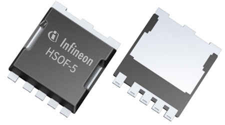
Infineon package reference image
New OptiMOS™ 5 40 V Mosfet in sTOLL Package (high power leadless package in 7x8 mm²) for future automotive applications (JEDEC: MO-319A, IEC: HSOF-5). The sTOLL package offers high current capability of 250 A and a footprint of 56 mm², smaller than DPAK's 65 mm². With Infineon’s advanced OptiMOS™ 5 technology, it delivers exceptional power density and efficiency, while maintaining Infineon’s renowned quality for robust automotive solutions.
Key Specifications
| Complete manufacturer part number | IAUA120N04S5N014AUMA1 |
|---|---|
| Manufacturer | Infineon Technologies |
| Description | New OptiMOS™ 5 40 V Mosfet in sTOLL Package (high power leadless package in 7x8 mm²) for future automotive applications (JEDEC: MO-319A, IEC: HSOF-5). The sTOLL package offers high current capability of 250 A and a footprint of 56 mm², smaller than DPAK's 65 mm². With Infineon’s advanced OptiMOS™ 5 technology, it delivers exceptional power density and efficiency, while maintaining Infineon’s renowned quality for robust automotive solutions. |
| Package / case | PG-HSOF-5-2 |
| Product category | Automotive MOSFET: 30 V to 800 V |
| Pins | 5 |
| Operating Temperature (manufacturer catalog) | -55 °C to 175 °C |
| Output Drivers (manufacturer catalog) | 1 |
| Polarity (manufacturer catalog) | N |
| QG (manufacturer catalog) | 62 nC |
| Technology (manufacturer catalog) | OptiMOS™5 |
| VGS(th) (manufacturer catalog) | 2.8 V |
| VGS(th) range (manufacturer catalog) | 2.2 to 3.4 V |
| QG [typ @10V] (manufacturer family record) | 62 nC |
| VGS(th) (manufacturer family record) | 2.8 V |
| VGS(th) minimum (manufacturer family record) | 2.2 V |
| QG maximum [typ @10V] (manufacturer family record) | 82 nC |
| RDS (on) maximum [@10V] (manufacturer family record) | 1.4 mΩ |
| VDS maximum (manufacturer family record) | 40 V |
| VGS(th) maximum (manufacturer family record) | 3.4 V |
| In stock | Contact for availability |
| Unit price | Request a quote |
| Lead time | To be confirmed |
Technical documentation and image source
Original manufacturer package appearance reference. Five exposed formed contacts on one edge, rear broad notched exposed metal and visible side metal. Original is two views, top and bottom. Rear metal is not nominal sixth pin; this -2 geometry is independent of prior -4. Original public manufacturer reference/render, not a current stock-lot photograph or guaranteed top marking. Only exact full OPN, complete mechanical suffix and nominal terminals listed; rear metal/pad is counted only as specified by nominal pins. Only surfaces actually depicted by the original are claimed. Individual dimensions, references, minima/maxima and nominal/general-tolerance values remain distinct. Exact complete OPN, full mechanical suffix, nominal terminals and own frozen datasheet define this association; only original depicted views, no electrical interchangeability or guaranteed marking.
Infineon package reference image for PG-HSOF-5-2. Confirm electrical pin functions in the datasheet. Actual lot appearance and top marking require current-lot confirmation.
Request a Quote
Why Source from CHIPER
- Quality inspection — every part is visually inspected and authenticity verified before shipment.
- Traceability — batch and date-code information provided on request.
- Shipping — worldwide shipping with major couriers (DHL / FedEx / UPS), fully insured.
- Payment — flexible terms including bank transfer (T/T) in major currencies.
- After-sales — dedicated support and RMA handling for every order.
Contact: xiaoqi@chiper-components.com · +86 18570555062